
AST-IR Workstation
NIR/SWIR Metrology & Inspection Workstation
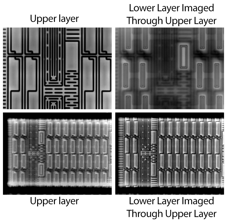
The NIR/SWIR Metrology & Inspection Workstation provides powerful subsurface imaging capabilities in a compact, versatile platform. This workstation penetrates through silicon and other wafer materials to reveal hidden structures, alignment issues, and defects with exceptional clarity. By harnessing advanced infrared imaging technology, the system delivers critical visualization for semiconductor, MEMS, and microelectronics applications where seeing beyond the surface is essential.

Product Highlights
The AST NIR/SWIR Microscope Workstation combines sophisticated optical systems with intuitive controls to address demanding inspection requirements. The system features recipe-selectable optical filters and programmable illumination controls to optimize contrast for a wide range of materials and applications.
The workstation architecture provides an ideal balance of performance and accessibility for research, development, and low-volume production environments. With its advanced vision tool library, the system enables precise geometric measurements and pattern recognition capabilities for comprehensive analysis.
- High-resolution optical system with NIR (400-1050nm) standard imaging and optional SWIR (900-1700nm) capabilities
- Advanced vision tools for executing pattern finding and geometric measurements
- Multiple objective options (5X, 10X, 20X, 50X, & 100X) for application-specific magnification
- Automated and programmable illumination, wavelength selection, and aperture diaphragm for optimal image contrast
- Digital contrast enhancement with recipe-controlled histogram adjustment
- Brightfield, darkfield, NIR, and SWIR illumination options for comprehensive imaging flexibility
Applications
- Inspection of bonded dies for layer alignment verification
- Wafer-to-wafer alignment analysis for 3D stacking applications
- Die-to-wafer bonding alignment verification
- Internal inspection and metrology on MEMS devices
- Semiconductor failure analysis
- Quality control for wafer bonding processes
- Subsurface inspection using NIR for low-doped materials and SWIR for highly doped wafers
Full Specifications
- 200MM X 200MM X-Y Travel ( 300mm x 300mm optional), 200mm Z Travel
- High-Resolution Optical System supporting
- 5X, 10X, 20X, 50X, & 100X BF & DF objectives
- Standard Video Auto-Focus
- Optional Tracking Laser Auto-Focus
- Brightfield, Darkfield, Kohler Illumination
- Optional Infrared (NIR & SWIR) Illumination with
5-Position Filter Wheel
- System can be configured with or without wafer loader
- Open cassette – wafers & film frames (50mm to 200mm)
- Custom die-level carrier & packaging assembles
Contact Sales
Our metrology systems can be fully customized to meet your requirements. If you have questions about our product offerings or capabilities, please contact us for more information.